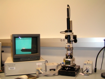
This microscope can be performed at both tapping and contact mode with highest resolution manufactured. With either the D-type (10x10x25µm) or the J-type scanner (125x125x5µm), images on both atomic and macroscopic scales can easily be obtained. The microscope performs the full range of SPM techniques to measure surface characteristics such as surface topography, elasticity, friction, adhesion, magnetic fields, and electrical fields. Surfaces of a wide range of materials, including conducting and non-conducting samples, can be examined with this microscope. The 2.5Å monolayer of GaN semiconductors can be easily resolved, as shown in the representative images. Attachments: optical viewing sytem, heating stage, signal access module, and vibration isolation tripod.
The second NanoScope is attached with a heater system that enables the measurements at elevated temperatures up to 150° C in a controlled environment. The temperature drift is +/- 0.025° C.
Lab:
Location:
1442 CNSI