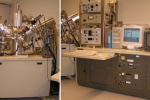
Instruments
Electron Microscopy
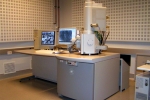
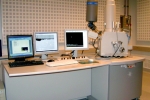
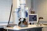
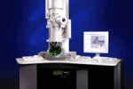
The electron microscope uses a focused electron beam energized up to 106eV to provide images and chemical information with very high spatial resolution. Since the short wavelength of electron beam and the successful development of low aberration electron optical lenses, the atomic resolution is routinely achievable for transmission electron microscope (TEM), as well as the resolution close to 1 nanometer for scanning electron microscope (SEM). The SEMs collect secondary and back scattered electrons to imaging the surface area, called SEI and BEI, while the TEMs mainly use the transmitted signals of a thin specimen. With a scanning device attached, a TEM can perform both transmission and scanning microscopy. Electron diffraction patterns can be obtained from TEM simultaneously as well as electron channeling patterns for SEM. Chemical analysis with a finely focused beam is another advantage of electron microscopy, such as electron dispersive X-ray (EDX) analysis and electron energy loss spectroscopy (EELS). The newly developed high coherent source, field emission gun of single crystal tungsten, has made high-resolution imaging and microanalysis with a beam size less than 1nm for TEM and close to 1nm for SEM possible. Now the power of electron microscopy has been widely used in almost every field of materials research, since it can provide both surface and microstructural information and the microscopes are getting more computerized.
Scanning Probe Microscopy
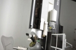
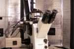
The scanning probe microscope (SPM) operates exactly as its name implies: a sharp tip is scanning on sample surface in a controlled contact or non-contact mode, and the signals carrying surface information are collected, processed and then plotted on a computer screen. The first base of SPM was scanning tunneling microscope (STM) that was invented 1982. After that, it has also been found not only the tunneling current, but also the atomic force and other kinds of interactions in between tip and sample surface can be probed. Therefore, the category of SPM samples is greatly extended from conducting to non-conducting or soft materials since the tip can work just in a near-surface scan. The name of scanning probe microscopy summarizes scanning tunneling microscopy, atomic force microscopy (AFM), scanning capacitance microscopy (SCM), magnetic force microscopy (MFM) as well as a range of other measuring techniques.
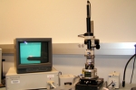
Scanning probe microscopes (STM/AFM)
Operation Modes: AC, Contact, LFM, Force, Nanolithography, EFM and Conductive AFM, and Low Force Indenter. Liquid AFM with closed fluid cell; Fluorescence filters.
Features: 90 μm travel in (x,y...
Operation Modes: AC, Contact, LFM, Force, Nanolithography, EFM and Conductive AFM, and Low Force Indenter.
Features: 90 micron travel in (x,y) and 15 micron in z; X-Y closed loop (non-linearity...
These SPMs have the similar functions in surface measurements with the Milti-Mode microscope as stated above. The major difference is that this microscope is designed for imaging a 6" wafer. A large...
This microscope can be performed at both tapping and contact mode with highest resolution manufactured. With either the D-type (10x10x25µm) or the J-type scanner (125x125x5µm), images on both atomic...
Surface Analysis Systems
X-ray Photoelectron Spectroscopy System
The Cameca IMS 7f Auto SIMS, combines the extreme sensitivity and mass resolution of earlier Cameca magnetic SIMS instruments with new features making operation easier and more consistent. The...
Purchased in 2001, the Kratos Ultra combines fast, high-sensitivity XPS (X-Ray Photoelectron Spectrometry) with a unique "real-time" imaging capability that allows us to quickly produce 2-dimensional...
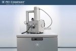
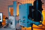
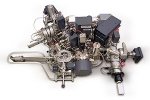
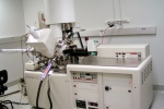
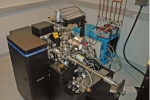
Focused Ion Beam Systems
DB235 is small stage system combining a Hexalens electron column and a Magnum ion column for failure analysis and high-end sample preparation. A Schottkey emitter is used for scanning electron...
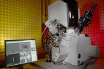
The instrument is equipped with an Elstar field emission SEM for nanometer resolution imaging and a Tomahawk FIB column operating from 30kV down to 500V. Ion currents range from 7pA, providing a...
Atom Probe Microscopes
Atom probe provides atomic -resolution, three-dimensional imaging, compositional imaging, and analyses. The Imago atom probe is used to analyze the structure and composition of materials for light...
Secondary Ion Mass Spectrometry System
Dynamic SIMS is used for depth profiling solid materials, allowing a determination of elemental composition as a function of depth. The key attributes of SIMS are its unparalleled sensitivity (...
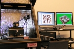
Electron Microscopy Simulation
Electron simulation software are loaded into a Mac and two PC computers that are open to users. Location: 1429 CNSI
Electron Flight Simulator (PC)
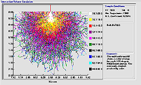
"Electron Flight Simulation" (Version 3.1) by Small World, Inc.
Environmental SEM analysis simulation and modeling software for Windows.
More details: www.small-world.net
jems Microscopy Simulation Software (PC)
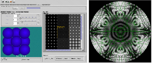
jems for Transmission Electron Microscopy (TEM) Simulation
Major functions: (1) Build up crystal structures; (2) Kinematical/dynamic electron diffraction (ED) calculation, including Kikuchi lines, HOLZ lines and CBED; (3) High resolution image interpretation; (4) TEM transfer function; (5) Tools for diffraction index, 3D crystallographic projection, etc.
Written by: Pierre A. Stadelmann; http://cimewww.epfl.ch/people/stadelmann/jemsWebSite/jems.html
CrystalKit and MacTempas (Mac)
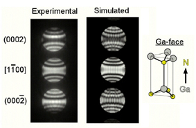
CrystalKit (version 1.8.3) Provider: Total Resolution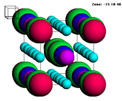 Crystallographic modelling of crystals, defects and interface. The program starts from single crystal data through a data-bank of the 230 spacegroups, and accepts up to 2 different crystalstructures for creating interface structures. The final structure generated by CrystalKit can be saved in a MacTempas file or an EMS supercell file for immediate simulation of diffraction patterns and High Resolution TEM images.
MacTempas (1.7.9) by Total Resolution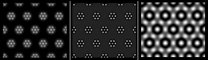 Multislice calculation of TEM diffraction and images. MacTempas is a full Macintosh application. Dynamical calculations of wavefunctions in thin crystal is carried out with defined slices and microscope parameters, and the output in different thickness can be controlled. Images as well as diffraction patterns at different conditions are shown in montage tables.
More details: www.totalresolution.com
Gatan DigitalMicrograph
DigitalMicrograph™ is Gatan Imaging Filter (GIF) system control software and also provides users to process and analyze images with TEM-oriented functions. For example, to perform Fourier transform (FFT) from either digital images or diffraction patterns, and the diffraction can also be masked with designed patterns. This program can also read images in some popular formats, such as TIFF, PICT, etc.
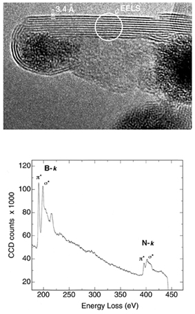
EL/P (v.2.1) is for acquiring and processing electron energy loss spectrum (EELS). In combine with DigitalMicrograph, the program can monitor the CCD-image of the spectra, as well as performing EELS mappings with selected edges of elements. Features of this EL/P include automated edge detection and identification, zero-loss peak tail deconvolution, thickness computation, and quantitative analysis with improved cross-section calculation. Processing spectrum with alignment and filter options, as well as Fourier transform (convolve/deconvolve) are available. Sample spectrum from a variety of compounds are provided.
More details: www.gatan.com
Desktop Microscopy (Mac)
"Desktop Microscopy" (Version 2.1) by Virtual Laboratory
Features: Crystallographic modeling of crystals, defects and interface; Stereographic Projection; Diffraction, Kikuchi map and CBED Bloch calculation; Dislocation imaging; Monte Carlo for electron diffraction of particles.
Electron simulation software are loaded into a Mac and two PC computers that are open to users. Location: 1429 CNSI
Electron Flight Simulator (PC)
"Electron Flight Simulation" (Version 3.1) by Small World, Inc.
Environmental SEM analysis simulation and modeling software for Windows.
More details: www.small-world.net